- 您现在的位置:买卖IC网 > Sheet目录1992 > CY28442ZXC-2 (Silicon Laboratories Inc)IC CLOCK ALVISO PENTM 56TSSOP
CY28442-2
..................... Document #: 38-07691 Rev. *B Page 18 of 19
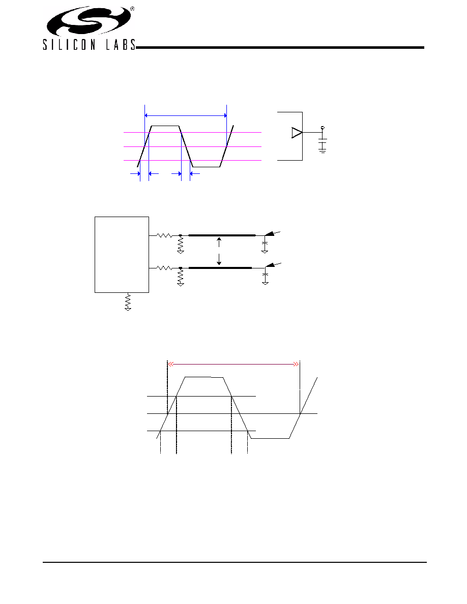
Test and Measurement Set-up
For PCI Single-ended Signals and Reference
The following diagram shows the single-ended PCI outputs.
The following diagram shows the test load configuration for the differential CPU and SRC outputs.
0V
3.3V
2.4V
0.4V
1.5V
tDC
Tf
Tr
Output under Test
Probe
Load
Cap
30
pF
Figure 14. Single-ended PCI Lumped Load Configuration
CP U T
CP UC
M e a s ur em e n t
Po in t
2pF
IR E F
M e a s ur em e n t
Po in t
2pF
SR C T
S RCC
D iffer e n tial
DO T 9 6 T
DO T 9 6 C
96 _100 S S C C
96 _100 S S C T
Figure 15. 0.7V Differential Clock Load Configuration
2.4V
0.4V
3.3V
0V
T R
T F
1.5V
3.3V sig na l s
T DC
-
Figure 16. Single-ended Output Signals (for AC Parameters Measurement)
发布紧急采购,3分钟左右您将得到回复。
相关PDF资料
CY28445LFXC-5
IC CLOCK CALISTOGA CK410M 68QFN
CY28446LFXC
IC CLOCK CALISTOGA CK410M 64QFN
CY28447LFXC
IC CLOCK CALISTOGA CK410M 72QFN
CY28547LFXCT
IC CLOCK CK505/410M INTEL 72QFN
CY28548ZXC
IC CLK CK505 960M/965M 64TSSOP
CY28551LFXC-3T
IC CLOCK INTEL/AMD SIS VIA 56QFN
CY28551LFXC
IC CLOCK INTEL/AMD SIS VIA 64QFN
CY2SSTV855ZXI
IC CLOCK DIFFDRV PLL DDR 28TSSOP
相关代理商/技术参数
CY28442ZXC-2T
功能描述:时钟发生器及支持产品 Calistoga RoHS:否 制造商:Silicon Labs 类型:Clock Generators 最大输入频率:14.318 MHz 最大输出频率:166 MHz 输出端数量:16 占空比 - 最大:55 % 工作电源电压:3.3 V 工作电源电流:1 mA 最大工作温度:+ 85 C 安装风格:SMD/SMT 封装 / 箱体:QFN-56
CY28442ZXCT
功能描述:IC CLOCK GEN ALVISO 56-TSSOP RoHS:是 类别:集成电路 (IC) >> 时钟/计时 - 时钟发生器,PLL,频率合成器 系列:- 产品变化通告:Product Discontinuation 04/May/2011 标准包装:96 系列:- 类型:时钟倍频器,零延迟缓冲器 PLL:带旁路 输入:LVTTL 输出:LVTTL 电路数:1 比率 - 输入:输出:1:8 差分 - 输入:输出:无/无 频率 - 最大:133.3MHz 除法器/乘法器:是/无 电源电压:3 V ~ 3.6 V 工作温度:0°C ~ 70°C 安装类型:表面贴装 封装/外壳:16-TSSOP(0.173",4.40mm 宽) 供应商设备封装:16-TSSOP 包装:管件 其它名称:23S08-5HPGG
CY28443
制造商:CYPRESS 制造商全称:Cypress Semiconductor 功能描述:Clock Generator for Intel㈢ Calistoga Chipset
CY28443-2
制造商:CYPRESS 制造商全称:Cypress Semiconductor 功能描述:Clock Generator for Intel㈢ Calistoga Chipset
CY28443-3
制造商:SPECTRALINEAR 制造商全称:SPECTRALINEAR 功能描述:Clock Generator for Intel㈢ Calistoga Chipset
CY28443OXC
制造商:CYPRESS 制造商全称:Cypress Semiconductor 功能描述:Clock Generator for Intel㈢ Calistoga Chipset
CY28443OXC-2
制造商:CYPRESS 制造商全称:Cypress Semiconductor 功能描述:Clock Generator for Intel㈢ Calistoga Chipset
CY28443OXC-2T
制造商:CYPRESS 制造商全称:Cypress Semiconductor 功能描述:Clock Generator for Intel㈢ Calistoga Chipset